The basic mechanism of hexagonal pattern formation in the 2 μm-thick elastic–plastic composite film. Top-view HRSEM image of an opening in the composite thin film.
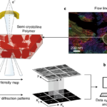
a, A converged sub-nm electron beam rasters over the sample, in this case a thin film of a semicrystalline semiconducting polymer, collecting local intensity measurements and local diffraction patterns. b, The big dataset obtained from the 4D-STEM is then synchronized and mined to provide orientation maps representing the direction of the brightest reflection at each point. c, The orientation map can be directly translated into flow-line maps that illustrate the orientation and extent of the molecular chains. Panel c reproduced from ref. 2, Springer Nature Ltd.
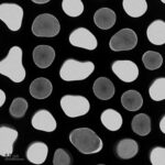
Surfactant-templated mesostructured silica formed within the pores of an alumina membrane
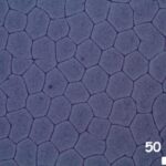
Microscope images of PCBM crystals in (a) P3HT/PCBM, and (b) P3HT/P3HT-TDO/PCBM thin films after annealing at 130 °C.
High resolution EFTEM composition mapping micrographs of a hybrid cross-sectioned FIB P3HT-b-PEO block copolymer and ZnO film. Zinc-rich domains are blue and sulfur-rich domains are red.
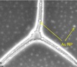
BSE SEM images of (a) Au NPs deposited by spin coating on a TiO2/ITO substrate; and (b) after the deposition of the overlying F127-directed TiOx/P3PBT mesostructure active layer. The Au NPs maintain their location and size and can be seen under the mesostructured layer and through a crack.
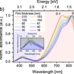
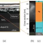
(a) Chemical structure, (b) normalized UV–vis absorption spectra, and (c) cross-polarized optical microscopy (CPOM) images of DPP-T-TT and corresponding films with different thicknesses. The high-energy transition in b (blue background) has predominantly π–π* character delocalized across both the donor and acceptor units (blue region in a). The low energy transition (red background in b) is assigned to the π–π* transition of the DPP unit (red region in a). The 0–0 and 1–0 vibronic transitions of the π–π* DPP transition are centered at 820 and 750 nm, respectively. The inset shows magnification of the high-energy transition revealing an increase in its intensity with film thickness. The dark areas in the cross-polarized POM images in (c) highlight polymer chains that are aligned along one of the two polarized directions, while the bright regions are associated with chains aligned close to ±45° (the angle for maximum transmission light intensity). The 16 nm thick film (bottom image) shows polymer chains elongated in extended fibrelike domains. In contrast, the image of the 100 nm thick film shows short flakelike birefringence structures.
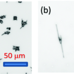
Chemical structures, device schematic and optical images of (a) semiconducting polymer DPP-T-TT, (b) PEG additive, (c) bottom-gate top-contact OFET, and (d) optical image of a substrate containing 20 devices with different channel lengths, L = 30, 40, 50, and 80 μm; and W = 1000 μm. Inset: microscopic image of a single OFET device (W/L = 1000/30).
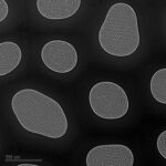
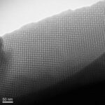
Transmission electron micrograph of F127 templated cubic mesostructure titania
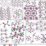
Structures of iodoplumbates based on protonated amides: (a) structure 1 based on protonated urea; (b) structure 2 based on protonated N-methyl-2-pyrrolidone; (c) structure 3 based on protonated dimethylacetamide; (d) structure 4 based on protonated diethylacetamide.
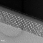
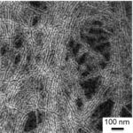
TEM image of a well-ordered PFO-incorporated P123- templated cubic composite film
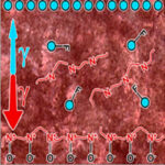
Schematic illustrations of the mechanisms that induce additive segregation to form interlayers in OPVs: (a) surface energy, (b) chemical interactions, (c) solubility, and (d) density or a concentration gradient.
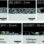
Cross-section HRSEM BSE micrographs of PCE11:PCBM films after thermal annealing at 130 °C for various time periods and VPI
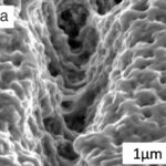
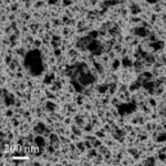
SEM image of porous WO3
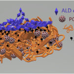
Atomic layer deposition of ZnO electron transporting layers directly onto the active layer of organic solar cells
Optical image of drying patterns observed in films deposited on glass substrates by dip-coating from WCl6:P123 precursor solutions with increasing polymer content. The WCl6:P123 wt. ratios in the precursor solutions is 2:1
(a) A SAXS pattern of F127-directed TiOx/P3PBT film with no Au particles; and (b) a SAXS pattern and (c and d) TEM images of F127-directed TiOx/P3PBT films with incorporated Au NPs. Dashed lines were added to highlight the nanoparticles in the TEM image.
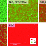
SEM images and EDS mapping of element C (in red) and Ni (in green) of thick NiOx:PEO films with different NiOx content. The cracks on the NiOx film are due to the slow drying process to obtain the desired high thickness required to perform the EDS analysis. The scale bar corresponds to 50 μm.
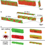
Tomographic reconstruction of selected PCE11:PCBM BHJs films from TEM and STEM tilt‐series showing the 3D‐spatial distribution of PCE11‐rich domains (green), PCBM‐rich domains (red), and the interface between them (yellow).
A schematic Illustration of P3HT:ICBA after low temperature ALD of ZnO, (left) low ICBA concentration, (right) ∼50% wt. ICBA.
HAADF STEM analysis of the hybrid ZnO and P3HT-b-PEO block copolymer self-assembly into fibers